
Why 90° PCB Angles Are Avoided

Better Angles. Better Flow. Better PCBs.
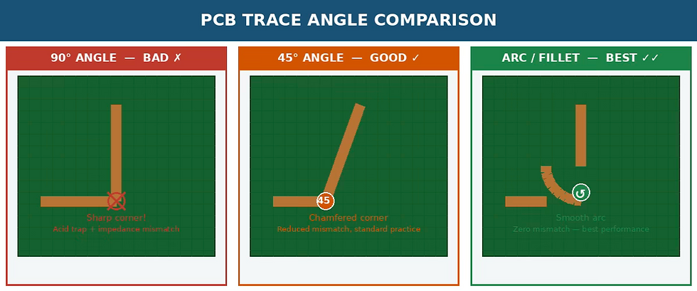
Figure 1: Visual comparison of 90°, 45°, and Arc/Fillet trace routing on a PCB
Introduction
PCB trace routing is far more than connecting dots on a board. Every bend, corner, and curve in a copper trace directly affects signal integrity, manufacturing yield, and long-term reliability. Among the most misunderstood aspects of PCB layout is the treatment of trace angles — specifically, why the industry standard strongly discourages routing at 90-degree angles.
Whether you are designing an Arduino shield, an industrial motor controller, or a GHz-class RF transceiver, understanding trace angle best practices is essential. This guide dives into the physics, manufacturing science, and industry standards that make 90° corners a red flag in professional PCB design — and shows you exactly how DipTrace PCB Design software helps you avoid them.
The 90° Angle Problem
At first glance, a 90-degree trace corner appears neat and compact. The routing looks grid-aligned and tidy. However, from a signal and manufacturing perspective, the 90° corner introduces several cascading problems that degrade board performance.
Acid Trapping During Etching
During PCB manufacturing, a chemical etchant removes unwanted copper. At a 90° inner corner, etchant gets physically trapped and cannot be rinsed away efficiently. This causes localized over-etching, which leads to:
Uneven copper removal — creating weak, thinned trace geometry
Reduced copper adhesion, causing delamination over time
Weak corners that crack under thermal cycling stress
Open circuits in severe manufacturing cases

Figure 2: Acid trapping mechanism at 90° vs clean etching at 45° corners — a key DFM risk
Non-Uniform Current Flow & Impedance Mismatch
Copper traces are not simple wires — they behave as transmission lines at high frequencies. At a 90° corner, the effective trace width momentarily increases by approximately 1.41× (diagonal of the square corner), creating a local impedance discontinuity. This mismatch causes partial signal reflection, increased inductance, higher EMI radiation, and distorted waveforms in digital and RF signals.
Signal Integrity Degradation
As PCB frequencies climb into the MHz and GHz range, these impedance mismatches become increasingly critical. A single 90° corner can introduce enough reflection to corrupt serial data signals, cause setup/hold time violations in digital logic, and push RF circuits outside their tuned band.

Figure 3: Signal waveform comparison — 90° routing causes ringing and reflections vs clean 45°/Arc signal
Mechanical Stress Concentration
Copper traces expand and contract with temperature during operation. The sharp inner corner of a 90° angle acts as a stress concentration point. Over hundreds of thermal cycles — common in automotive, aerospace, and industrial electronics — micro-cracks initiate at these corners, eventually causing intermittent or permanent failures that are notoriously difficult to diagnose in the field.
Angle Comparison: 90° vs 45° vs Arc/Fillet
Not all trace angles are equal. The table below summarizes the performance differences across the three common routing strategies:

The minimum acceptable standard for professional PCB design is 45° chamfered routing. For high-speed digital, RF, aerospace, automotive, and medical-grade boards, smooth arc or fillet routing is strongly recommended.
Industry Standard – IPC – 2221B

Beyond IPC-2221B, related standards including IPC-6012 (qualification for rigid boards) and IPC-A-600 (acceptability of printed boards) all reinforce the same design discipline: avoid sharp internal corners in copper traces.
Where it Matters More
While 90° angles are always discouraged, certain board categories demand especially strict adherence:
High-Speed Digital Circuits
Boards carrying signals above 100 MHz — DDR memory, PCIe, USB 3.x, LVDS differential pairs — are highly sensitive to impedance discontinuities. Even small reflections can cause bit errors, requiring expensive re-spins or over-engineered signal conditioning to compensate.
RF & Analog Circuits
In RF design, trace geometry directly affects matching networks, antenna performance, and filter response. A 90° corner introduces parasitic capacitance of 0.01–0.05 pF — negligible at audio frequencies, but significant at 2.4GHz (WiFi/Bluetooth) or 5GHz (WiFi 6 / 5G NR) where a few femtofarads shift the entire impedance match.
Power Electronics
High-current power traces experience significant Joule heating. A 90° corner's thinned geometry creates a hot spot that reduces current-carrying capacity and accelerates electromigration. Power distribution networks should use wide filleted traces or copper pours.
Aerospace, Automotive & Medical PCBs
These safety-critical applications operate across extreme temperature ranges (-55°C to +125°C) with strict reliability requirements. Thermal cycling fatigue at 90° corners is a primary long-term failure mechanism — which is why all three industries mandate IPC-2221B compliance by contract.
Routing the Right way in DipTrace
DipTrace is engineered from the ground up to help designers produce professional, IPC-compliant PCBs with confidence. Here is how its tools directly address the 90° angle problem:

Figure 4: DipTrace PCB Layout — key features for IPC-compliant 45°/Arc trace routing
45° and Free-Angle Routing Modes
DipTrace's PCB Layout editor provides multiple routing angle modes accessible from the Route menu. The 45° mode automatically constrains traces to chamfered bends — the most common professional routing standard. Free-angle mode allows any angle, enabling true arc-shaped routing for sensitive RF and high-speed traces.
Real-Time DRC (Design Rule Check)
DipTrace's real-time DRC engine continuously monitors your layout for violations as you route. You can define custom rules to flag 90° angles as errors, ensuring that even in complex multi-layer boards, no sharp corners slip through to fabrication.
Differential Pair Routing
High-speed differential pairs (USB, LVDS, PCIe, HDMI) are especially sensitive to impedance mismatches. DipTrace's differential pair router maintains equal trace lengths and consistent spacing through bends — automatically applying 45° geometry to keep the pair compliant and matched.
3D Preview & Gerber Export
DipTrace's integrated 3D Preview lets you visually inspect trace routing quality across the full board before export. All corner geometries are visible in the 3D model, giving you a final DFM check before generating IPC-compliant Gerber files.
Best Practices Summary

Figure 5: PCB trace angle guidelines and IPC-2221B key rules at a glance

Conclusion
The 90-degree PCB trace angle is not just an aesthetic preference — it is a documented engineering risk that affects acid trapping during manufacture, signal integrity at high frequencies, EMI compliance, mechanical reliability over thermal cycles, and adherence to IPC-2221B standards.
The fix is straightforward: route with 45-degree chamfers as a minimum and prefer smooth arcs or fillets wherever signal quality and reliability matter most. DipTrace gives you the routing tools, real-time DRC, and professional 3D verification workflow to make IPC-compliant trace routing the default — not the exception.
Good PCB design is all about smooth paths and smart choices.
Designed Better with DipTrace |
Every routing decision matters. DipTrace gives you the tools to route traces at correct angles, apply arc and fillet corners, and run real-time Design Rule Checks — ensuring your PCB meets IPC standards before it reaches the fab. Download Free: diptrace.com/download |
DipTrace is a professional EDA/CAD software suite for schematic capture and PCB layout design. Trusted by engineers worldwide, DipTrace provides an intuitive interface, powerful autorouter, comprehensive component libraries, real-time DRC, 3D preview, and full Gerber output. Available free with upgrade paths for professional and enterprise use.
Comments